Nanostructured carbon materials have existed as a prominent area of materials research for over two decades, from the discovery of Buckminsterfullerenes to carbon nanotubes and more recently graphene, including freestanding carbon nanosheets with thickness less than 1 nm. Our research group has pioneered a technique to grow a unique covalently bonded graphene-carbon nanotube hybrid material using plasma-enhanced chemical vapor deposition (PECVD) in a single step. We are working to understand the relationships between deposition parameters and morphology, and subsequently structure-property relationships for high graphene edge density nanomaterials ranging from multi-walled carbon nanotubes to various CNT-graphene hybrid materials and carbon nanosheets comprised of few-layered graphene. Application areas for these materials include charge storage as supercapacitor electrodes, field emission devices, neural stimulation electrodes, lithium ion batteries, transparent conductive electrodes, flexible electronics, and carbon nanotube field effect transistors.
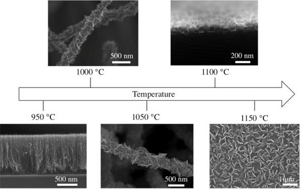
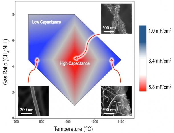
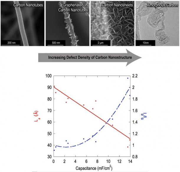
Figure 1 illustrates the effect of deposition temperature on nanostructure morphology, varying from carbon nanotubes (CNTs) to graphenated carbon nanotubes (g-CNTs), and finally carbon nanosheets (CNSs) comprised of few-layered graphene (FLG). The CNS morphology may be seen in more detail in Figure 2 by scanning electron microscopy and transmission electron microscopy. g-CNTs perform particularly well as supercapacitor electrodes due to their combination of the high charge storage capacity of the FLG sheets and the high surface area CNT scaffold (Figure 3). Through studying these high edge density nanostructures, a relationship was elucidated between the defect density of carbon nanostructures and their specific capacitance, which is the first observation of its type to span a wide variety of nanostructured carbons (Figure 4).
Carbon nanomaterial application areas:

Figure 1: The film morphology varies dramatically from the CNT structure at 950 °C, to g-CNTs at 1000 °C and 1050 °C, to CNSs at 1100 °C under otherwise constant growth conditions.

Figure 2: (a) Cross sectional and (b) Top-view SEM image of carbon nanosheets. (c) HR-TEM micrograph of a single nanosheet with two graphene layers, as seen by the two parallel fringes.

Figure 3: In the temperature range associated with the deposition of graphenated carbon nanotubes, a local capacitance maximum is observed. g-CNTs perform particularly well as supercapacitor electrodes due to their combination of high charge-density graphene edges and a high surface area CNT scaffold.

Figure 4: As the crystallite size of the nanostructure is reduced and defect density is increased, an increase in specific capacitance is observed independently of changes in total surface area.
Recent Publications
Ubnoske, SM; Raut, AS; Parker, CB; Glass, JT; Stoner, BR(2015)."Role of nanocrystalline domain size on the electrochemical double-layer capacitance of high edge density carbon nanostructures" MRS Communications.5(02): 285- 290 More info
Henry, PA; Raut, AS; Ubnoske, SM; Parker, CB; Glass, JT(2014)."Enhanced electron transfer kinetics through hybrid graphene-carbon nanotube films." Electrochemistry Communications.48: 103- 106 More info
Ubnoske, SM; Raut, AS; Brown, B; Parker, CB; Stoner, BR; Glass, JT(2014)."Perspectives on the Growth of High Edge Density Carbon Nanostructures: Transitions from Vertically Oriented Graphene Nanosheets to Graphenated Carbon Nanotubes." The Journal of Physical Chemistry C.118(29): 16126- 16132 More info
Zhang, S; Kang, P; Ubnoske, S; Brennaman, MK; Song, N; House, RL; Glass, JT; Meyer, TJ(2014)."Polyethylenimine-Enhanced Electrocatalytic Reduction of CO 2 to Formate at Nitrogen-Doped Carbon Nanomaterials" Journal of the American Chemical Society.136(22): 7845- 7848 More info
